
Cutting or Removing or Marking Wafer Tape
Applications for Sem...Description
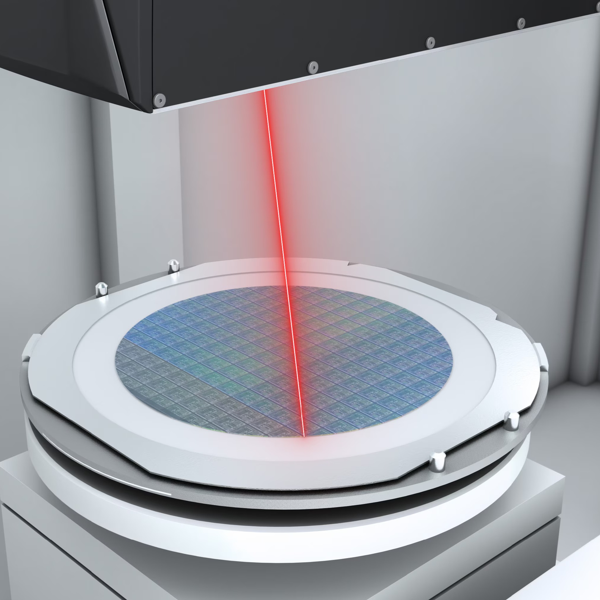
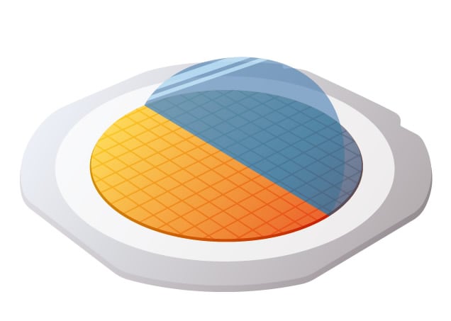
Before milling the bottom surface, the wafer tape applied to protect the surface of the wafer is cut. Before removal, the wafer tape is irradiated with a laser to reduce adhesion. Identification marking is also applied to the cut ribbon before wafer cutting is carried out.
Actions
Share
Related Products
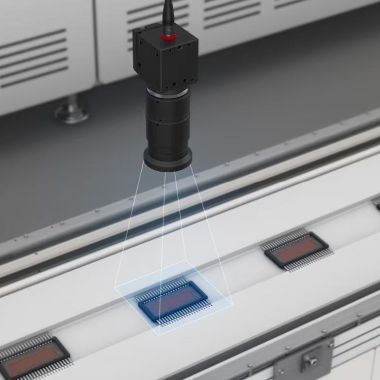
Power Semiconductor Wire Inspection
<p>The use of high-resolution cameras ensures greater clarity when examining cable details.</p>
OCR with Electronic PCB
<p>While marking inspections with conventional systems means capturing separate images, processing time can be increased by capturing the entire field of view at once with a high pixel camera.</p><p><img src="https://www.keyence.co.id/img/application/90634.jpg"></p>
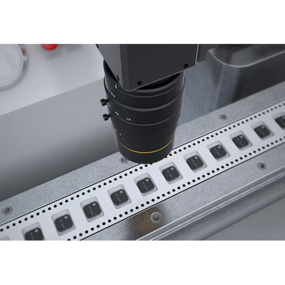
Product Type Differentiation or 2D Identification of IC Packages
<p>Reads 2D characters/codes marked with a laser on the surface of the IC chip. A single machine vision can recognize both characters, such as part numbers and 2D codes simultaneously.</p><p style="text-align: center;"><strong>OK</strong></p><p><img src="https://www.keyence.co.id/img/application/90600.jpg"></p><p style="text-align: center;"><strong>NG</strong></p><p><img src="https://www.keyence.co.id/img/application/90601.jpg"></p>