
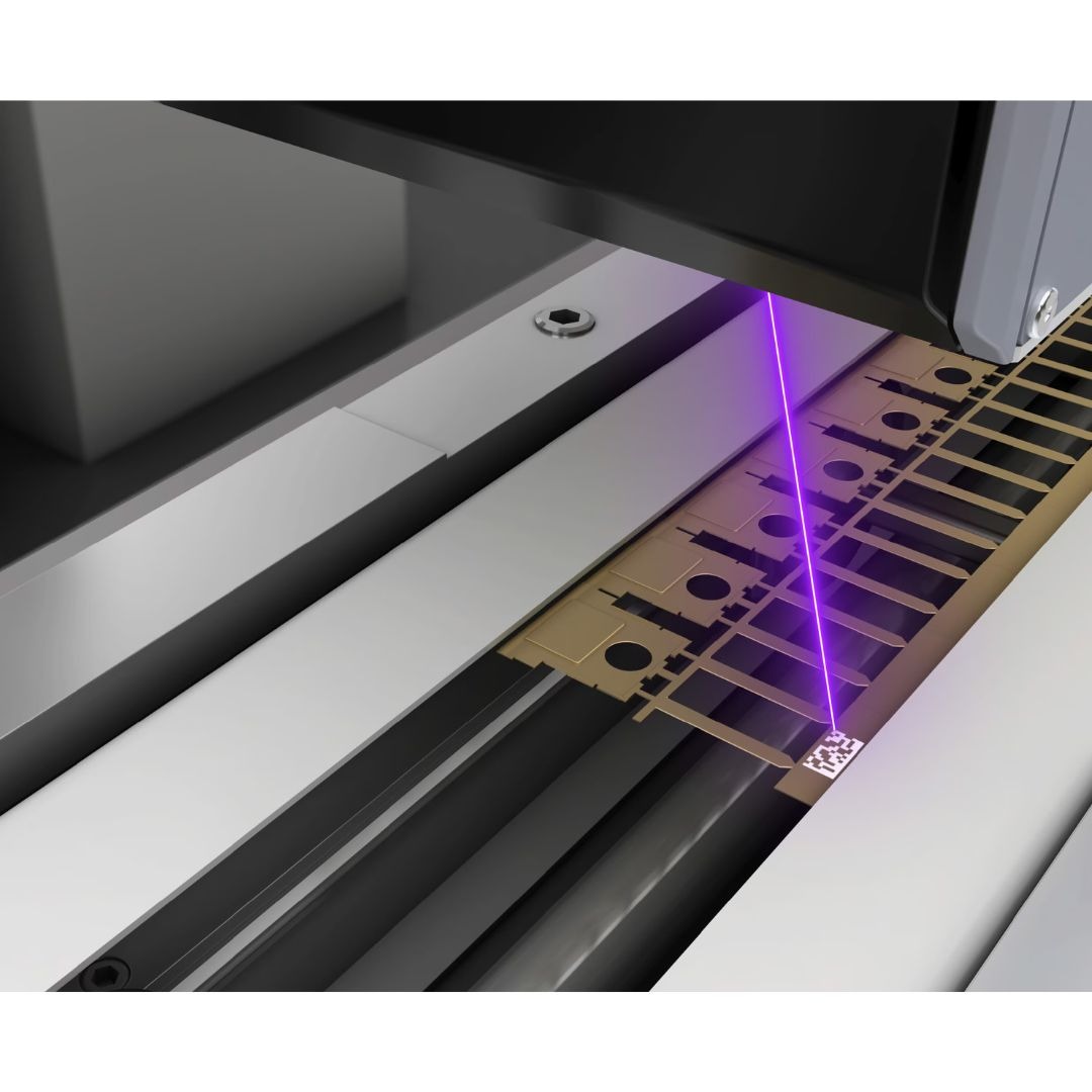
Marking on Lead Frame or DBC Substrate
Applications for Sem...Description
To ensure stable code reading, even when marked in confined spaces, KEYENCE markers allow users to select the optimal 2D code marking pattern taking into account the material and surface conditions of their targets. This makes it possible to mark 2D codes that can be read immediately after coating is completed.
Actions
Share
Related Products
Power Semiconductor Wire Inspection
<p>The use of high-resolution cameras ensures greater clarity when examining cable details.</p>

OCR with Electronic PCB
<p>While marking inspections with conventional systems means capturing separate images, processing time can be increased by capturing the entire field of view at once with a high pixel camera.</p><p><img src="https://www.keyence.co.id/img/application/90634.jpg"></p>

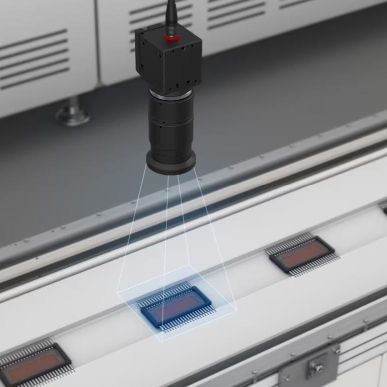
Product Type Differentiation or 2D Identification of IC Packages
<p>Reads 2D characters/codes marked with a laser on the surface of the IC chip. A single machine vision can recognize both characters, such as part numbers and 2D codes simultaneously.</p><p style="text-align: center;"><strong>OK</strong></p><p><img src="https://www.keyence.co.id/img/application/90600.jpg"></p><p style="text-align: center;"><strong>NG</strong></p><p><img src="https://www.keyence.co.id/img/application/90601.jpg"></p>