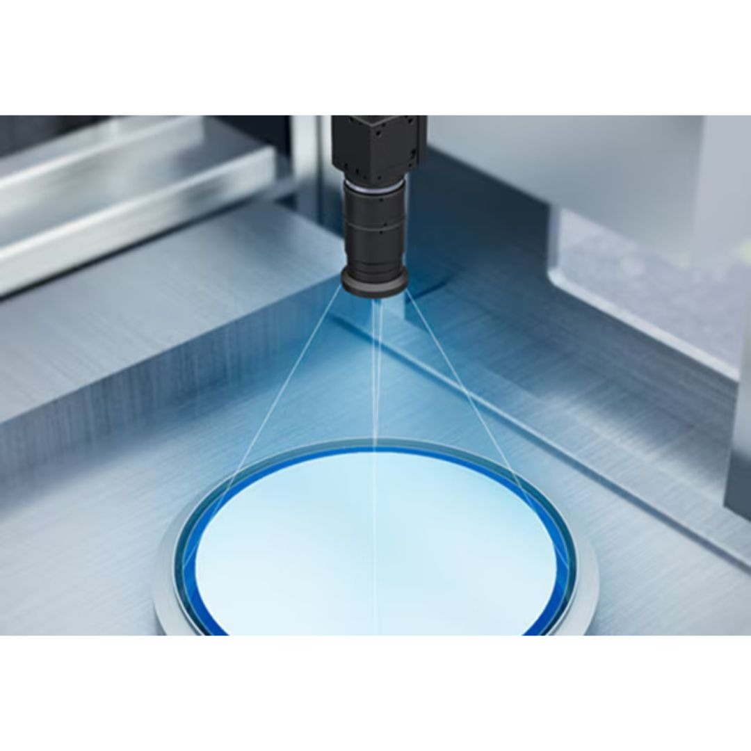
Checking Wafer Position
Applications for Sem...Description
While conventional systems are required to capture discrete images to ensure high resolution, wide-area imaging allows capturing the entire field of view at once to increase processing time.
Actions
Share
Related Products

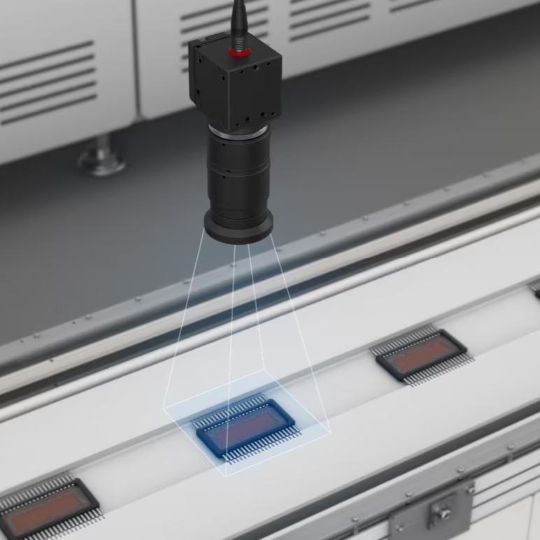
Power Semiconductor Wire Inspection
<p>The use of high-resolution cameras ensures greater clarity when examining cable details.</p>

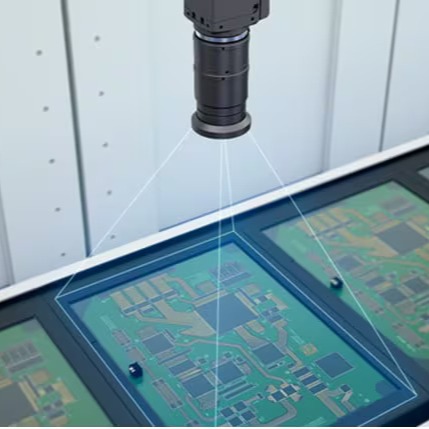
OCR with Electronic PCB
<p>While marking inspections with conventional systems means capturing separate images, processing time can be increased by capturing the entire field of view at once with a high pixel camera.</p><p><img src="https://www.keyence.co.id/img/application/90634.jpg"></p>

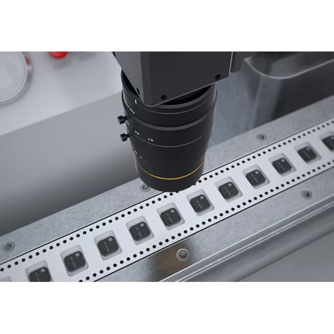
Product Type Differentiation or 2D Identification of IC Packages
<p>Reads 2D characters/codes marked with a laser on the surface of the IC chip. A single machine vision can recognize both characters, such as part numbers and 2D codes simultaneously.</p><p style="text-align: center;"><strong>OK</strong></p><p><img src="https://www.keyence.co.id/img/application/90600.jpg"></p><p style="text-align: center;"><strong>NG</strong></p><p><img src="https://www.keyence.co.id/img/application/90601.jpg"></p>
